Diamonds are a qubit’s best friend — and the Quantum Prairie is building them a supply chain
Diamonds are key materials for certain quantum technologies, and collaboration among Midwest companies that manufacture and process them is advancing the national supply
For centuries, diamond has been the ultimate symbol of permanence and luxury. But in the field of quantum information technology, the value of a diamond has nothing to do with its sparkle on a ring.
Instead, quantum scientists value it for its flaws: defects that can be used as qubits, the building blocks of quantum technologies. Diamonds are especially useful as quantum sensors, which are expected to be among the first commercially viable segments of quantum technology.
Manufacturing diamonds with the particular defects needed for quantum technology can be a difficult, expensive process. But an emerging ecosystem of companies, all connected to the Illinois-Wisconsin-Indiana region, is developing the partnerships and workflows needed to build one of the nation’s first robust quantum diamond supply chains.
This regional momentum is anchored by five Chicago Quantum Exchange (CQE) corporate partners whose diverse and complementary strengths span the entire production lifecycle: Great Lakes Crystal Technologies (GLCT) and WD Advanced Materials, which specialize in high-purity diamond growth; K1 Semiconductor and staC12, startups whose innovative techniques provide the essential wafer production and thin-film integration needed for chip-scale devices; and Applied Materials, a global leader providing the industrial infrastructure to bridge laboratory breakthroughs with mass manufacturing. Exemplifying the complementary nature of their specialties, GLCT and K1 Semiconductor are developing a partnership.
In addition, several CQE corporate partners, including Dirac Labs, FemtoSenseLabs, and SandboxAQ, are integrating diamond into their quantum sensors.
“When you have an ecosystem like this, where all of these players have come together, you can tap into this network and find people working on similar things,” said Debarati Mukherjee, vice president of product development at GLCT. “You can find partners that have the technology or services you need, or want to develop, and we’ve been introduced to companies in Wisconsin and Indiana that way where we might not have found each other otherwise.”
This regional push is anchored by The Bloch Quantum Tech Hub, a cross-sector coalition led by the CQE. Designated as a US Tech Hub by the Economic Development Administration, The Bloch is competing for federal funding to build the US a domestic quantum technology supply chain by integrating manufacturers and quantum developers into a unified ecosystem that enables the sector to scale. For diamond-based technologies, such systems could solve the complex production bottlenecks that have historically slowed their adoption.
“The Bloch leverages the deep partnerships that the CQE has fostered across industry, government, and academia to address critical gaps in the quantum ecosystem, including our lack of an at-scale domestic quantum supply chain,” said David Awschalom, the Liew Family Professor of Molecular Engineering and Physics at the University of Chicago and the director of the CQE. “The collaboration among suppliers of diamond-based technologies offers an example of what we can accomplish on a broader scale with federal funding. Their cooperative work is forming the basis of an integrated supply chain for diamond — something we hope to build and scale across the entire quantum technology sector.”
The “ultimate semiconductor”
Semiconductors are extremely important in the electronics industry, where they make up most of the foundational components of our everyday devices like laptops and smartphones. Silicon is the most common semiconductor due to its low cost and significant abundance (second-most abundant element in the Earth's crust); but diamond, also a semiconductor, performs vastly better than silicon in nearly every measurable way, including thermal conductivity, power efficiency, and physical resistance and reliability.
“Diamond is the ultimate semiconductor,” said Paul Quayle, vice president of research and development at GLCT. “But when you try to make that into a device, like electronics or for quantum technologies, oftentimes the quality of the material just isn’t high enough to exploit it for the performance that you need.”
The challenge is twofold: quality and cost. Quantum applications — including computing, networking, and sensing — require the diamond to have very particular defects, called “vacancy centers.” These are what can store and manipulate quantum information, and the manufacturing process must account for their creation as the fundamental units of diamond-based quantum technology.
In addition to quality concerns, diamond is significantly more expensive and difficult to manufacture than silicon, even though the process to make it was first developed in the 1950s.
But the ability to manufacture quantum-quality diamond at larger scales has dramatically improved over the past few years, Quayle says, and it’s driving “a tremendous amount of growth on both the market pull side and the manufacturing side.”
“Scaling the synthesis and integration of diamond can supercharge the next generation of quantum and electronic technologies,” said Alex High, chief science officer at staC12 and associate professor of molecular engineering at the University of Chicago Pritzker School of Molecular Engineering (UChicago PME). "Building a collaborative, regional supply chain in the Midwest ensures the transition from lab-scale physics to field-deployed quantum sensors isn’t throttled by material scarcity."
Building a regional supply chain
GLCT, K1 Semiconductor, and staC12, which are based in the Midwest, and WD Advanced Materials and Applied Materials, which are connected to the Midwest through CQE partnership, are leveraging these improvements in different ways to scale manufacturing systems and meet market demand.
“Today, a lot of diamond quantum technologies work with very small crystals,” said John Ciraldo, chief technology officer at WD Advanced Materials, which manufactures diamond for advanced technical, scientific, and industrial applications including quantum. “But when it scales up, it’ll look like a semiconductor process. There's a lot of technology that needs to be either developed or modified from the semiconductor industry to be amenable to quantum technologies. And that's a big emphasis right now.”
K1 Semiconductor, a deep tech startup developed at UChicago PME by Connor Horn and Xella Doi, uses a breakthrough semiconductor wafer-splitting “spalling” technology that could improve the cost-efficiency and scalability of semiconductor manufacturing.
“We need to make diamond growth more economically viable and also enable larger-scale wafers,” said Sagar Kumar Seth, co-founder of K1.
The K1 wafer-splitting (spalling) process allows for the repeated use of a single semiconductor substrate—up to 20 cycles—by removing ultra-thin layers from the surface.
(Credit: K1 Semiconductor)
K1 is partnering with GLCT to scale the production of quantum-grade diamond wafers in the Midwest. The two companies have collaborated on funding proposals under which GLCT would manufacture bulk diamond that K1 would split into wafers and templates, using their proprietary wafer spalling technology. K1 would then pass the templates back to GLCT to produce more bulk diamond in an integrated manufacturing cycle. The process is still being piloted.
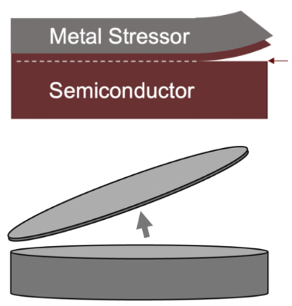
staC12, another startup out of UChicago PME, specializes in not only synthesizing high-performance thin-film diamond, but integrating thin-film diamond onto substrates like silicon, sapphire, and lithium niobate. This illustrates another challenge in high-tech diamond manufacturing — once you have the diamond, how do you integrate the hardest material in the world into electronic chips to make devices that work?
“All of modern technology is made of material heterostructures: layers of different materials,” said Avery Linder, co-founder and CEO of staC12, “and diamond is not easy to work with. If you want diamond in the next generation of technologies, you need a way for diamond to integrate in with other materials in these heterostructure devices.”
Applied Materials, a leading materials engineering company, is also working in this area: using techniques from the semiconductor industry to integrate diamond-based technology into the layered heterostructures that make up much of today’s advanced technology.
“The diamond is the active heart of the device,” said Robert Visser, vice president in the office of the CTO at Applied Materials, “but you need to get optical signals in and out, and possibly do electrical measurements as well. Infrastructure for that is what we provide.”
Why diamond?
Qubits tend to be extremely fragile, losing their quantum information with any disturbance. But diamond defect qubits are surrounded by the hardest natural material on Earth, which provides a very effective shield: its high thermal conductivity efficiently dissipates heat, its electrically insulating properties keep electrical noise away, and its stiff, durable structure protects it from other environmental disturbances. This allows diamond qubits to keep their quantum information for longer, and at higher temperatures than other types of qubits that may need to be kept colder than outer space.
The ability of diamond defects to maintain quantum information for longer periods of time makes them particularly good quantum sensors. These sensors are most often used for the ultra-precise measurement of magnetic fields, which has applications in navigation and mining. But magnetic fields can be used as proxies for a variety of different measurements: for example, attaching a magnetic atom to a drug molecule could allow a quantum sensor to track it through a cell.
Diamond also makes an excellent candidate for quantum memory, used in quantum communication or computing. While quantum sensing applications of diamond are already being commercialized, quantum communication and computing applications are developing slower; but Ciraldo is confident they’ll mature.
“Diamond is going to be the second implementation [of quantum computing],” he said, “the later implementation where it goes beyond what you can do with other systems.”